SoftBank and Intel Unveil Energy-Saving AI Memory Chip
In a significant move for artificial intelligence infrastructure, SoftBank and Intel have announced their collaboration on developing an innovative memory chip specifically designed for AI applications. The new technology promises to slash power consumption by approximately 50% compared to existing solutions.

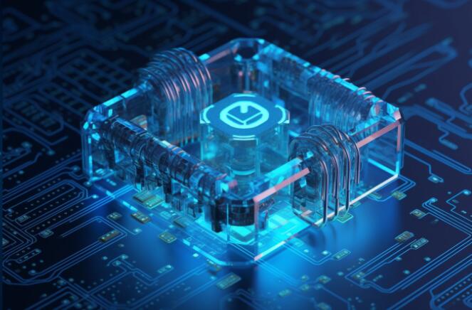
Image Source Note: Image generated by AI, licensed by MidJourney
The partners are designing a novel stacked DRAM chip with wiring architecture that differs fundamentally from current high-bandwidth memory (HBM) standards. This breakthrough could transform energy efficiency in data centers handling intensive AI workloads.
A newly established company called Saimemory will spearhead the project, focusing on chip design and intellectual property management while outsourcing manufacturing to specialized foundries. The ambitious timeline calls for prototype completion within two years, followed by mass production evaluation. Commercial availability is targeted for the late 2020s.
SoftBank leads the ¥10 billion (approximately $64 million) investment with a ¥3 billion commitment. The project has attracted interest from prominent research institutions including RIKEN and Kobe Precision Machinery, who may contribute both funding and technical expertise. Government support is also being sought to accelerate development.
The timing couldn't be better as global demand for AI computing power surges. Data centers face mounting pressure to improve performance while reducing environmental impact. SoftBank plans to deploy these chips in its own AI training facilities, potentially setting new benchmarks for sustainable operations.
What makes this development particularly noteworthy? Unlike incremental improvements, the partners aim for a fundamental redesign of memory architecture. Their approach addresses one of AI's most pressing challenges - the staggering energy requirements of modern machine learning systems.
Key Points
- Joint venture targets 50% reduction in memory power consumption for AI applications
- New stacked DRAM design breaks from conventional HBM architecture
- ¥10 billion project led by SoftBank with Intel's technical expertise
- Commercial deployment planned for late 2020s
- Potential game-changer for sustainable AI infrastructure


